MEASURING INSTRUMENT
IMAGE INSPECTION EQUIPMENT
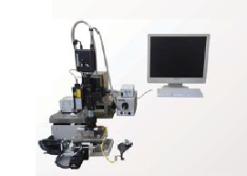
Image inspection equipment system
We select image processing equipment, including lighting, and provide GUI solutions tailored
to image processing, control, and requests.
In addition to image processing, we also support the construction of automatic systems
embedded in the equipment.
Examples of actual cases
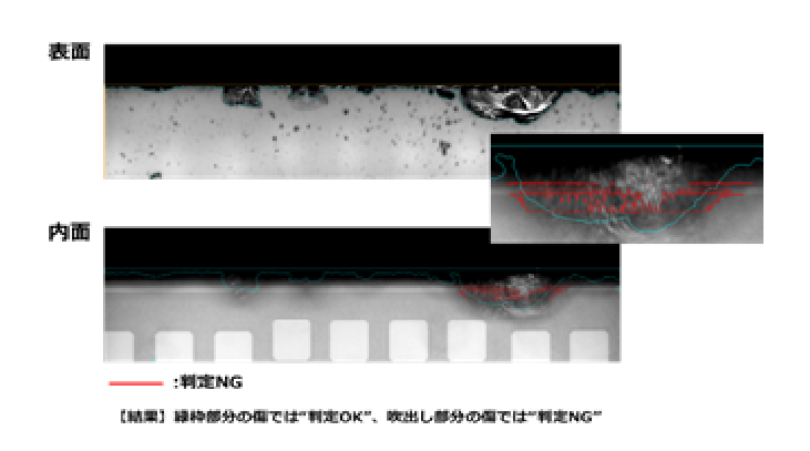
Near-infrared image inspection
【Feature】
It is possible to inspect metal wiring and die bonding inside
semiconductor devices such as silicon wafers, chips, MEMS,
and CSP.
【Target material】
Si (silicon) , GaAs (gallium arsenide) , ceramic
Product Videos
Tester & Image inspection equipment lineup
LD tester
LX72 series
Including the unique measurement of
LD device
FFP measurement NFP measurement Pulse measurement
Optical measurements are also available.
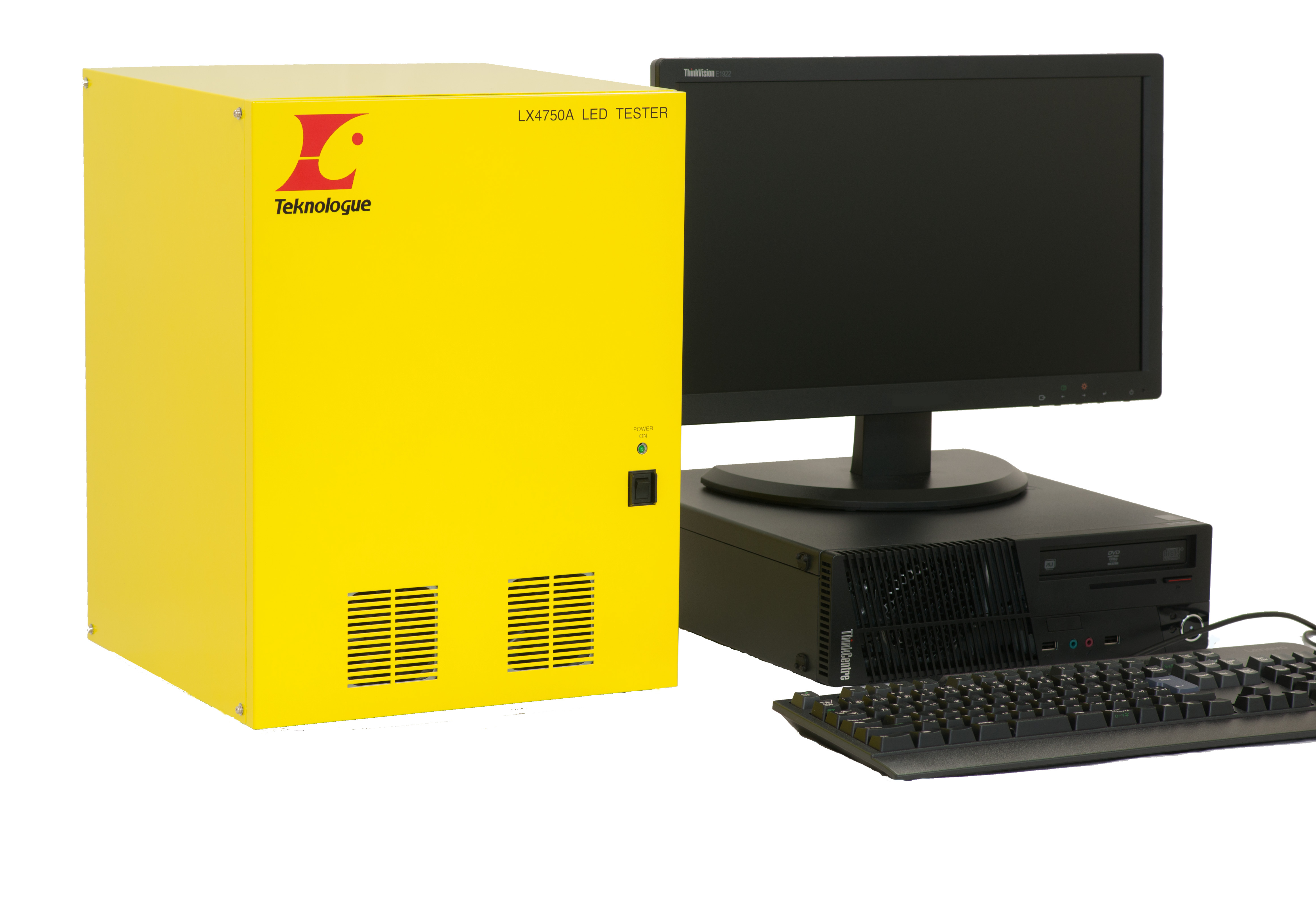
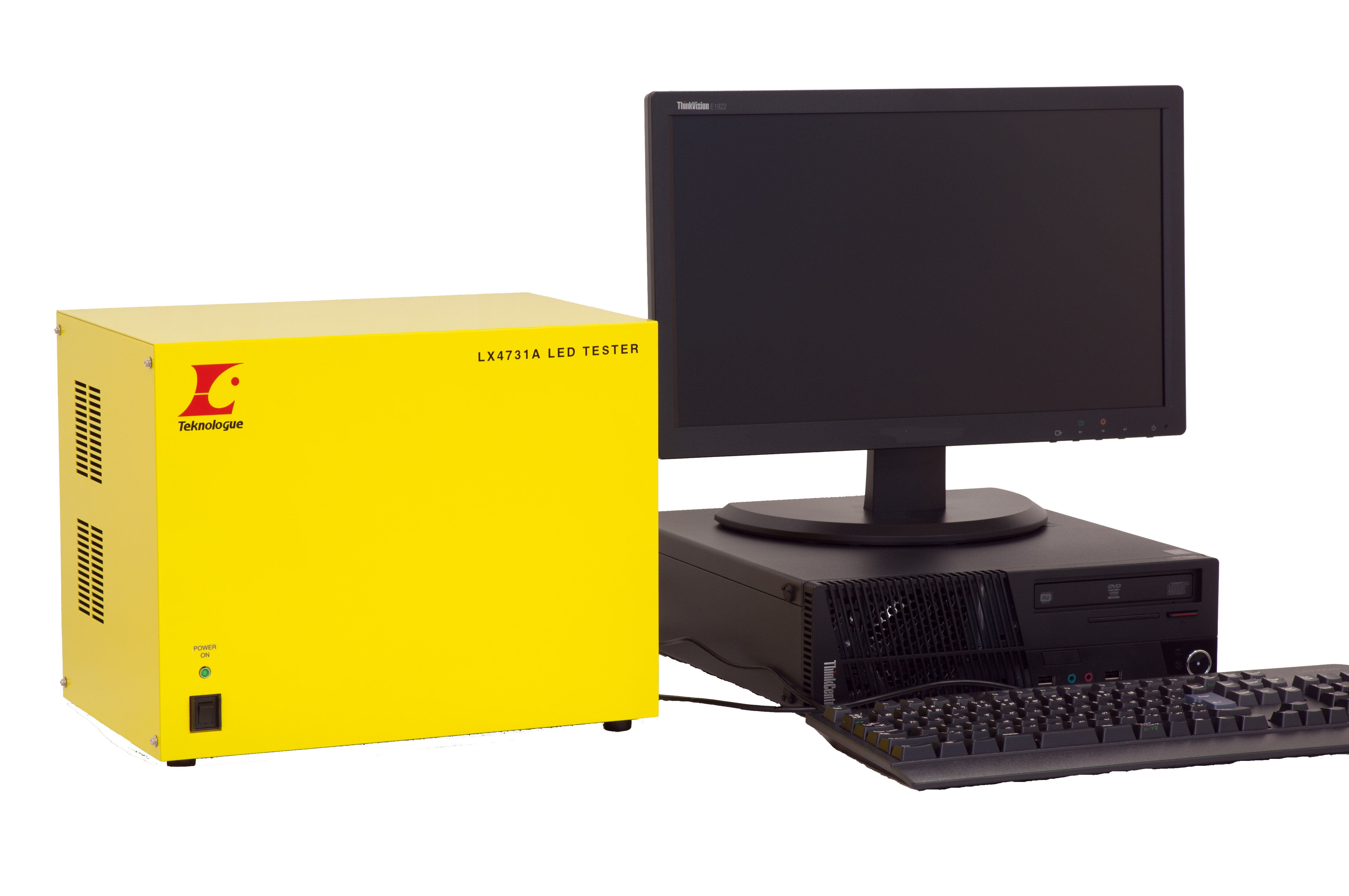
LED tester
LX47 series
In addition to the unique measurement
of LED devices, optical measurement in
the infrared, visible, and ultraviolet
regions is possible.
CONTACT
For document requests and inquiries, please contact us using the email form below or by phone.
Click here for inquiries by phone
+81-428-31-8211